
1
Pulse Width Modulation
Module Descriptions & PIL Examples using the
F28069M LaunchPad Board.

Copyright © 2015 Altair Engineering, Inc. Proprietary and Confidential. All rights reserved.
Topics:
• PWM & Duty Cycle
• ePWM Block – Modules
• Time Base
• Action Qualifier
• Deadband
• Event Time
• Solenoid Modeling, Simulation, Transfer Function Approximation, Processor in the Loop (PIL) Simulation
(requires F28069M board to be attached)
• Motor Modeling, Dynamics, Time Constant
• Using the eCap block to record PWM Carrier Period and Frequency (Example requires the F28069M board to be
attached)
2
Copyright © 2015 Altair Engineering, Inc. Proprietary and Confidential. All rights reserved.
PWM Basic Terminology
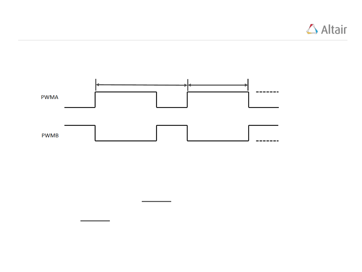
3
The “ePWM” block (“Embedded/F280x”) produces two PWM signals (PWMA and PWMB). These
control signals are always opposite each other; when one is high (On), the other is low (Off):
Tpwm
tOn
Tpwm = Carrier Period(sec)
Duty Cycle =
tOn
Tpwm
Fpwm = Carrier Frequency, Hz =
1
Tpwm
Three Important PWM Features:
On value
On value
Off value
Off value
Copyright © 2015 Altair Engineering, Inc. Proprietary and Confidential. All rights reserved.
PWM Generation
4
In an embedded application, the target processor produces pulses from a Time Based Clock (TBCLK).
The Time Based Clock can run at the CPU speed or a fraction of it. Pulses produced by the TBCLK
are counted as they occur forming a staircase signal whose count value at any time is monitored by a
Time Based Counter (TBCTR). When the TBCTR reaches a preset value named the Time Base
Period (TBPRD), the counter resets itself to 0 and the staircase signal repeats. PWM signals are
produced based when the TBCTR equals a Compare (CMP) value.
time
time
PWM
On value
Off value
TBCTR
(counts)
CMP value
5
4
3
2
1
0
Time Based Clock (TBCLK), (sec)
TBPRD value
Copyright © 2015 Altair Engineering, Inc. Proprietary and Confidential. All rights reserved.
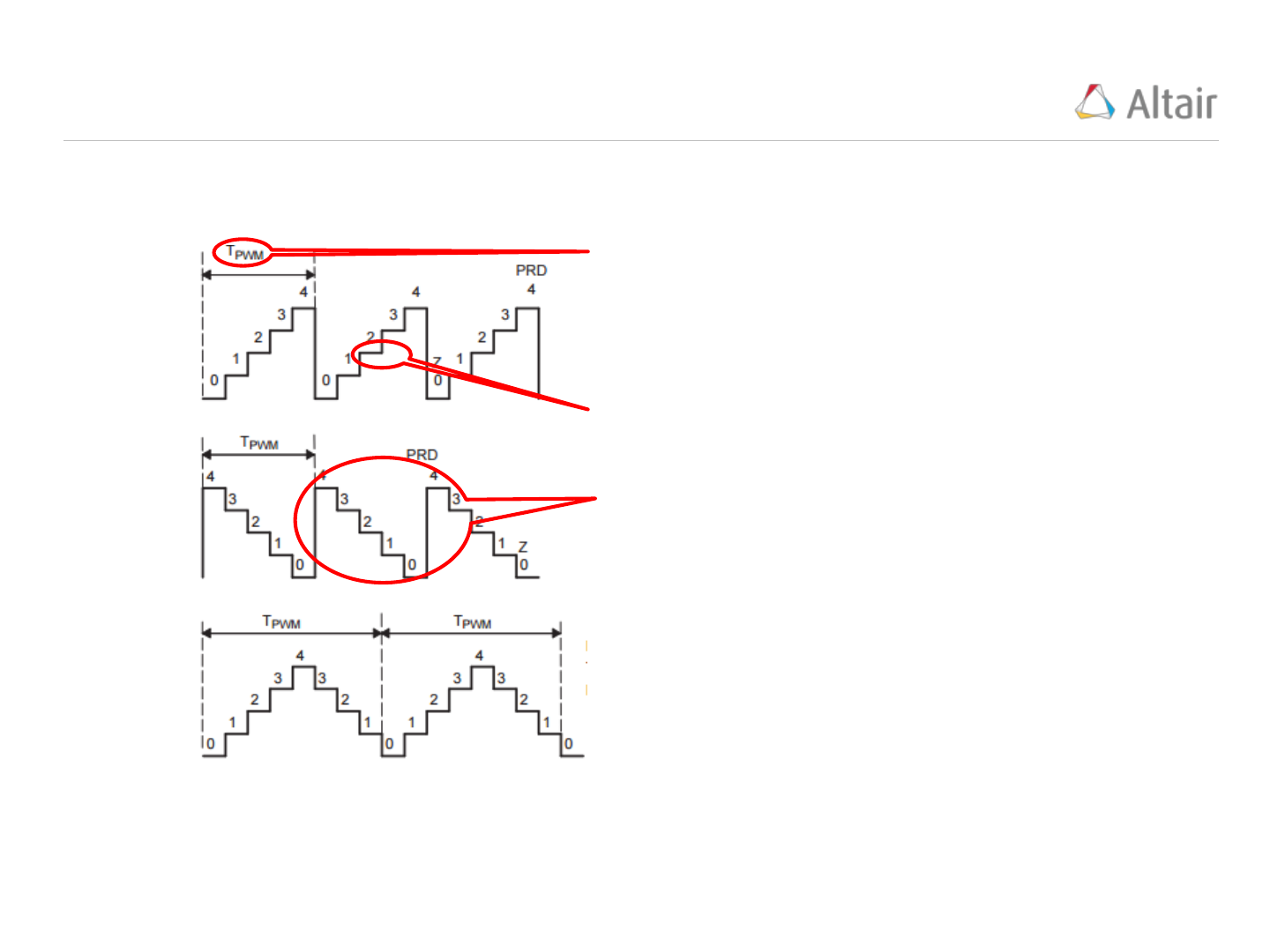
PWM Count Mode, Period, and Frequency
5
Most target processors support three Count Modes; Up Count, Down Count, and Up/Down Count:
Up
Count
Mode:
Down
Count
Mode:
Up/Down
Count
Mode:
Tpwm is the PWM
Carrier Period (sec),
Fpwm is the PWM
Carrier Frequency
(Hz).
Tpwm is approx.
twice the value for
the Up/Down
Count Mode
compared with the
Up or Down Count
Modes
Each step occurs at
a clock tick.
Timer Period is the
number of steps in
one Carrier Period
Tpwm = (TBPRD + 1) * TBCLK
Tpwm = 2*TBPRD* TBCLK
Tpwm = (TBPRD + 1) * TBCLK
Fpwm = 1/Tpwm
Fpwm = 1/Tpwm
Fpwm = 1/Tpwm

Copyright © 2015 Altair Engineering, Inc. Proprietary and Confidential. All rights reserved.
PWM Resolution
6
The resolution, n, of a PWM generator is equal to the number of Time Based pulses present in the
PWM period expressed as a number of bits.
Resolution expressed as a number of bits:
Number of Time Base pulses per PWM period =
For example, a 20kHz PWM signal is to be generated using an 80MHz CPU. The Time Based Clock
(TBCLK) is set to 1/80Mhz and the resolution is calculated as:
The High Resolution Timer option, if available on your hardware, decreases the TBCLK to a value of
150e-12 seconds. This is particularly useful if your application requires a high PWM frequency
(NOTE: 250kHz and greater is considered to be a high PWM frequency).
Copyright © 2015 Altair Engineering, Inc. Proprietary and Confidential. All rights reserved.
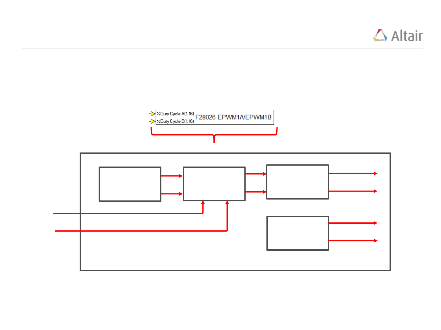
DCB
DCA
VisSim ePWM Block
7
The VisSim ePWM block (below) is a two channel device. It has two Duty Cycle (DC) inputs and
produces two PWM output signals and two Start of Conversion (SOC) signals. The channels are
referred to as “A” and “B”. The DC inputs are fractions in 1.16 format. The PWM and SOC signals are
sent directly to hardware pins. They are accessible to your VisSim model using an “Extern Read”
statement.
SOCA
PWMB
PWMA
SOCB
Action Qualifier
Module
Deadband
Module
Time Based
Module
Event Time
Module
The ePWM block consists of four key Modules; (1) Time Based, (2) Action Qualifier, (3) Deadband,
and (4) Event Timer. Each Module is described in this document.
Copyright © 2015 Altair Engineering, Inc. Proprietary and Confidential. All rights reserved.
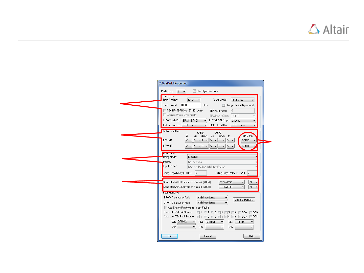
VisSim PWM Block – Module Properties
8
The VisSim ePWM block (“Embedded/Piccolo/ePWM”) property window is used to configure the PWM
Modules.
Time Base Module: Define the type of
count and Period
Action Qualifier Module: Define when the
PWM cycles and the PWM output Pin
Deadband Module: Define deadband to
prevent “shoot-through” and polarity
PWM Output Registers
Event Time Module: Define the SOC
signals
SOC Outputs
Copyright © 2015 Altair Engineering, Inc. Proprietary and Confidential. All rights reserved.
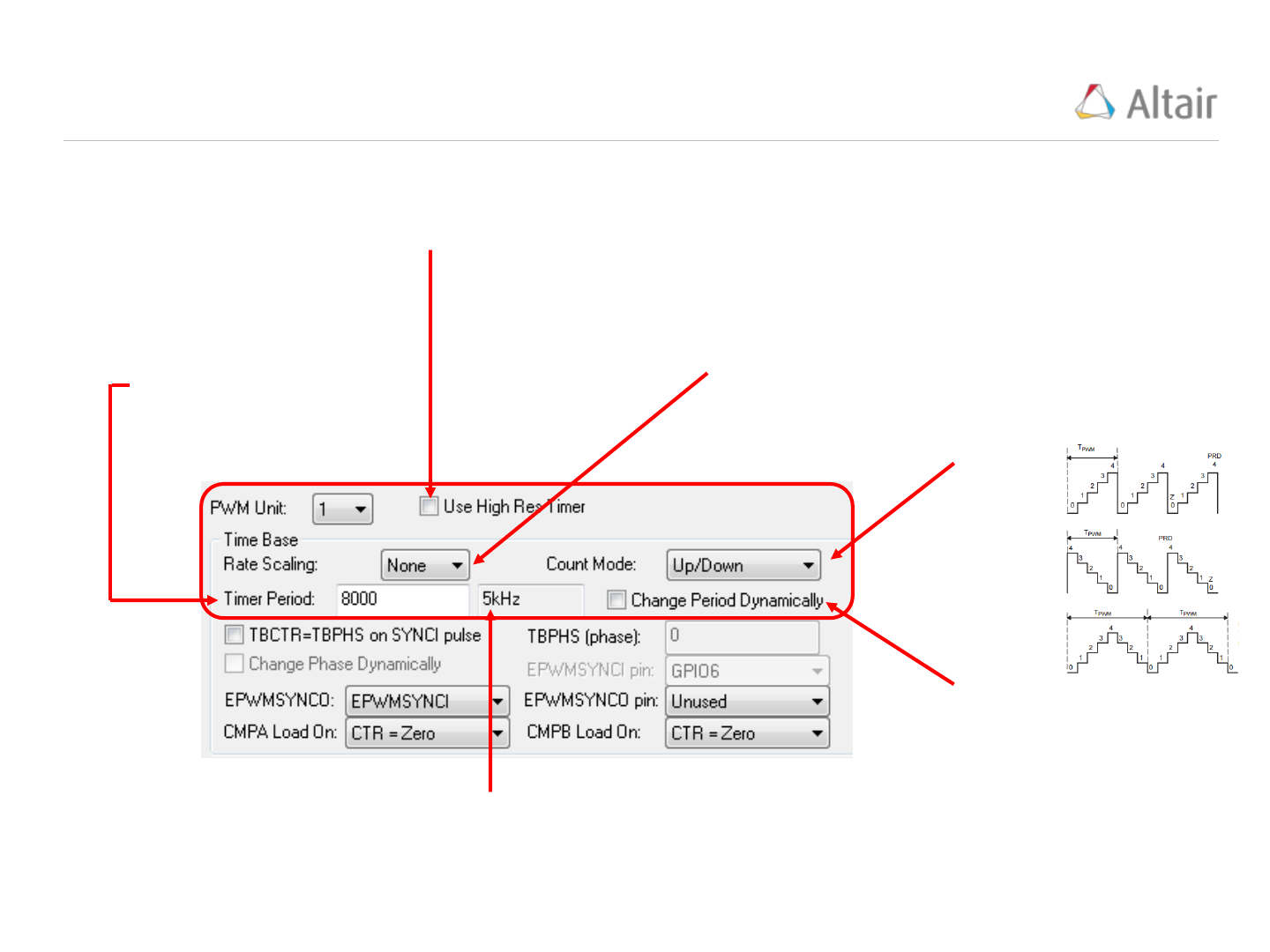
VisSim ePWM – Basic Time Base Module Configuration:
9
User select: Set the
TBPRD = # clock ticks
per PWM period.
VisSim calculates the PWM Carrier frequency
(Fpwm) based on the Timer Period, Count Mode,
and Rate Scaling.
3 Count
Modes:
Sets the TBCLK = k/CPU clock speed
(Hz), where k is selected from the
dropdown menu. Note: “None” means
k=1.
The basic “Time Base” Module features of the ePWM (“Embedded/F280x”) block are located in the
“Time Base” frame of the ePWM properties window.
Explained on the
next slide
Sets the TBCLK = 150e-12 seconds (approximately) for high
frequency PWM applications (typically > 250kHz)
Copyright © 2015 Altair Engineering, Inc. Proprietary and Confidential. All rights reserved.
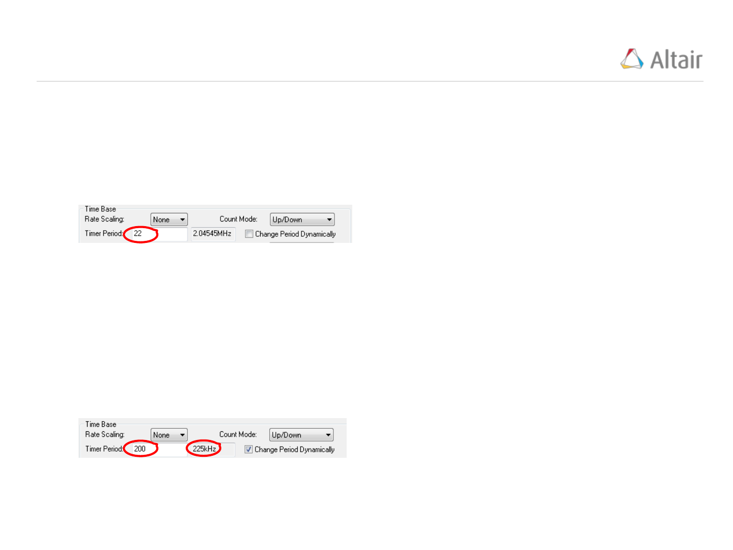
Change Period Dynamically Option
10
Based on the ON and OFF times selected, the PWM Period is calculated as 500nsec and the PWM
Carrier Frequency is calculated as 1/500nsec = 2MHz.
In some situations it is not possible to create the desired PWM Carrier Frequency from the integer “Timer
Period”. Suppose we wanted to create a PWM signal with a minimum 25nsec ON time and 475nsec OFF
time. The “Count Mode” is set to “Up/Down”. The CPU Speed is 90MHz and the TBCLK = 1/90MHz.
Since the “Timer Period” MUST be an integer
value, it is not possible to achieve the desired
2MHz PWM Carrier Frequency. (Here the best
we can do is set “Timer Period” = 2 to achieve
2.04545MHz)
To solve this problem, select the “Change Period Dynamically” option which adds a “Period(1,16)”
input pin to the PWM block. This pin accepts a user defined “Fractional Period Multiplier”
constant that is calculated as follows:
After some experimentation adjusting the “Timer
Period” value, we select a value of 200 which
produces a PWM Carrier Frequency of 225kHz.
Since 225k/2M = .1125 is a rational fraction
between 0 and 1, we will use this “Timer Period”
value and a “Fractional Period Multiplier” set to
.1125 to achieve the 2MHz PWM Carrier
Frequency.
Experiment with the “Timer Period” value until you obtain a value that produces a PWM Carrier
Frequency, F, such that F/2MHz is a rational fraction between 0 and 1 (Note: 2MHz is the desired
PWM Carrier Frequency). The “Fractional Period Multiplier” is set to this rational fraction.

Copyright © 2015 Altair Engineering, Inc. Proprietary and Confidential. All rights reserved.
PWM Frequency Selection Issues:
11
Interference with Mechanical System Frequency: Generally dominant mechanical frequencies are in the
200Hz or less range. PWM frequency should be selected at least 10x the dominant mechanical
frequency. This is normally not a limiting factor.
Power Loss: In a motor, torque is proportional to the average current. Consider a motor with a torque
constant k driven by a constant current source,
and by a PWM current source that ranges from 0 to
and has a Duty Cycle, DC. To achieve the same torque, the following is true:
The PWM driven motor requires
more current than the constant
current motor to develop the
same torque.
Heat: In a motor winding there is always a small resistance, R. As current is passed through
the winding resistance,
watts of energy is transferred from electrical to heat energy. For
a PWM current signal with a period, T, on-time, tOn, Duty Cycle, DC, and ranging from 0 to
, the
value is calculated as:

Copyright © 2015 Altair Engineering, Inc. Proprietary and Confidential. All rights reserved.
PWM Frequency Selection Issues:
12
For a 0 to
PWM signal, power loss through a resistor, R, is calculated as:
For a constant current signal of value
, power loss through R is:
As DC decreases, more and more power is lost through the
resistance to heat when using a PWM signal compared to a
constant signal of the same average value.
Switching Losses: An ideal switch is either fully on or off which means it never dissipates any power.
Real switches don’t switch instantaneously, they have a transition time during which they dissipate power.
The transition time is usually fixed per edge. For example, using a switch that requires a 1 microsecond
transition time in a 25kHz PWM (40 microsecond period) means that the transition time is 1/40 of the
total. If the PWM frequency were increased to 250kHz (4 microseconds), this ratio would increase to ¼
which would significantly and adversely affect performance.
Vibration and Noise: An electric motor uses wire coils to produce magnetic force. Every length of wire
in the motor undergoes lateral movement proportional to the current being passed through it. When the
current is cycled, i.e. a PWM signal, the movement becomes a regular vibration audible to the human
ear. Since the range of human hearing is generally considered to be 20Hz to 20kHz, PWM frequency is
often selected to be 20kHz or greater to eliminate audible noise being produced.
Resolution: Normally a resolution of 10 bits (1/1024 = .001) is adequate. Based on your CPU speed
and PWM period, confirm your resolution is adequate. If not consider using the “High Resolution Timer”,
adjusting the PWM period, overclocking, or moving to a faster CPU.
Copyright © 2015 Altair Engineering, Inc. Proprietary and Confidential. All rights reserved.
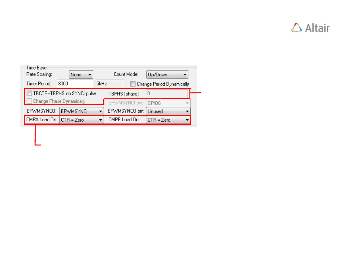
Advanced Time Base Module Configuration:
13
TBPHS: is a count offset value (to produce
a phase shift)
TBCTR = TBPHS on SYNC1 pulse: When
checked, the TBPHS count offset value is
added to TBCTR when a SYNC1 pulse
occurs.
Change Phase Dynamically: Adds an input
pin to the PWM block which accepts a
fractional value that is multiplied by the
“Timer Period” and assigned to “TBPHS”.
The advanced “Time Base” Module features of the ePWM (“Embedded/F280x”) block are located in the
“Time Base” frame of the ePWM properties window
Specify the condition when to load the CMPA and
CMPB values. Choices are [Zero, Period, Period
or Zero, and Immediate]. Normally “Zero” is
selected.
Copyright © 2015 Altair Engineering, Inc. Proprietary and Confidential. All rights reserved.
Advanced Time Base Module Configuration -
Synchronization:
14
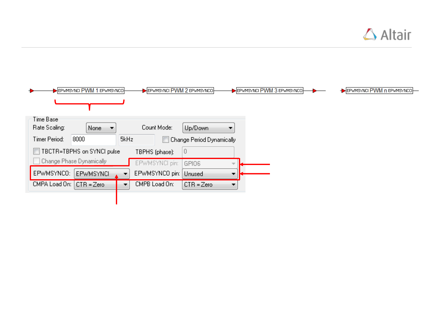
The operation of PWM modules can be synchronized to operate as a single system when needed using
hardware pins named EPWMSYNCI (input) and EPWMSYNCO (output).
There are 4 selectable synchronizing actions that can be applied to the
EPWMSYNCO output signal:
EPWMSYNCI: This sets EPWMSYNCO = EPWMSYNCI
TBCTR = zero: This sets EPWMSYNCO = 1 when the TBCTR (time based
counter) = 0
TBCTR = CMPB: This sets EPWMSYNCO = 1 when the TBCTR = CMPB
None: This sets EPWMSYNCO =0 always
…
Input pin
Output pin
Copyright © 2015 Altair Engineering, Inc. Proprietary and Confidential. All rights reserved.
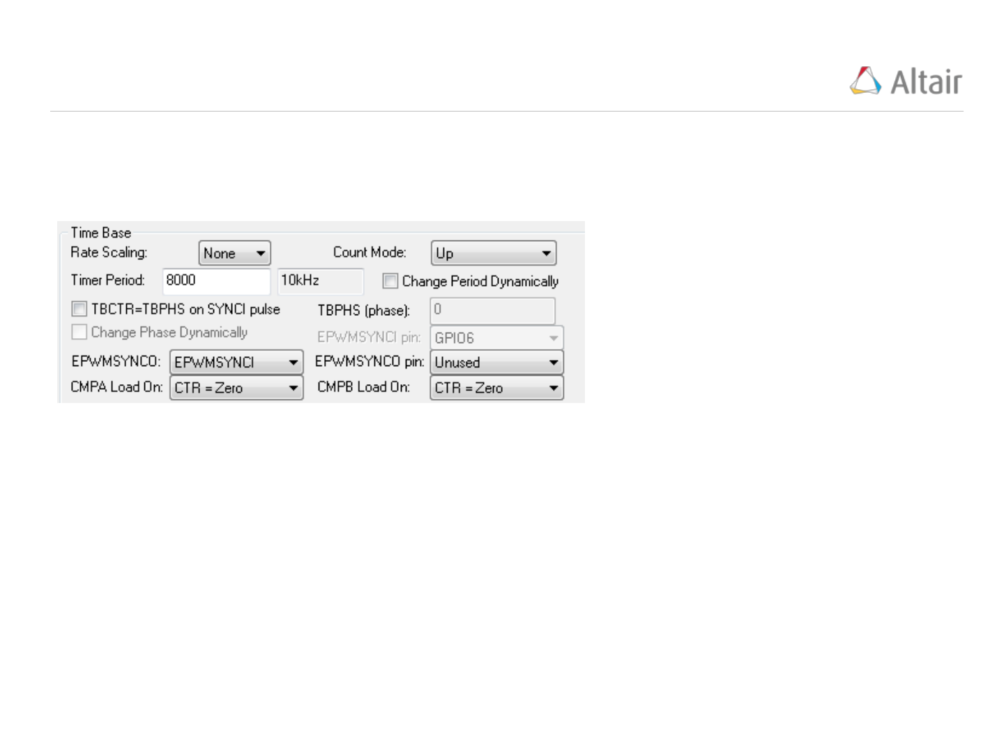
VisSim PWM – Time Base Setup Example 1
15
Example 1:
Setup the PWM to produce a 10kHz carrier frequency with “Count Mode” set to “Up. The CPU Speed
is 80MHz.
Step 1: Experiment with “Timer Period” until 10kHz Carrier Frequency is
obtained.
NOTE: CPU Speed = Timer Period * Carrier Frequency
NOTE: there are 8000 discrete levels of duty cycle in this configuration
Copyright © 2015 Altair Engineering, Inc. Proprietary and Confidential. All rights reserved.
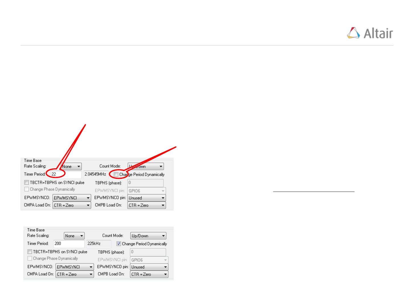
VisSim PWM – Time Base Setup Example 2 (1/3)
16
Based on the ON and OFF times provided, the Carrier Period is calculated as 500nsec OR equivalently,
the Carrier Frequency is 2MHz.
Example 2:
Setup the PWM to produce a 25nsec ON and 475nsec OFF signal with “Count Mode” set to
“Up/Down”. The CPU Speed is 90MHz.
“Timer Period” MUST be an integer
value, we cannot achieve the desired
2MHz Carrier Frequency.
To solve this problem, use the “Change Period Dynamically” option
which allows you to define a “Fractional Period Multiplier” and send to
the “ePWM” block through the “Period” input pin.
Operation:
New Carrier Frequency =
New Timer Period =
Setting the “Fractional Period Multiplier” = .1125, these settings
become:
New Carrier Frequency = 225kHz/.1125 = 2MHz
New Timer Period = 200 * .1125 = 22.5
Copyright © 2015 Altair Engineering, Inc. Proprietary and Confidential. All rights reserved.
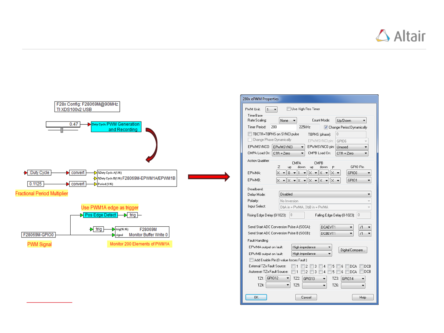
VisSim PWM – Time Base Setup Example 2 (3/3)
18
Debug Model:
Debug Model
Plot x-Range Calculation:
200 points are recorded in the buffer.
PWM frequency = 2MHz = 500nsec
Fractional Period Multiplier = .1125
xMax = 200 * 500e-9 * .1125 = 1.125e-5 seconds
Simulation Setup:
TimeStep = .01 seconds
End = 20 seconds
Sample Rate = 225kHz
NOTE: the actual sample rate is 225kHz/.1125 =
2MHz
Copyright © 2015 Altair Engineering, Inc. Proprietary and Confidential. All rights reserved.
PWM Events & Actions
19
time
TBCTR
(counts)
CMP value
5
4
3
2
1
0
TBPRD value
Zero (Z) Event:
TBCTR = 0
Up Event:
TBCTR = CMP while increasing
Period (P) Event:
TBCTR = TBPRD
Down Event:
TBCTR = CMP while decreasing
At each Event, any of four Actions can be performed. These actions provide a means to define the
PWM edges:
X = Do Nothing
0 = Force the PWM value to 0 (Off Value)
1 = Force the PWM value to 1 (On Value)
T = Toggle the PWM value
if the PWM value = 1, Toggle will set it = 0 and if the PWM value = 0, Toggle will set it = 1
The Duty Cycle input value is
converted to a CMP value.
As the TBCTR pulse counter
increments from 0 to TBPRD,
it passes through the CMP
value.
Similarly, when the TBCTR is
reset to 0, it also passes
through the CMP value.
These four Events, Z, Up,
Down, and Period are shown
(right):
Copyright © 2015 Altair Engineering, Inc. Proprietary and Confidential. All rights reserved.
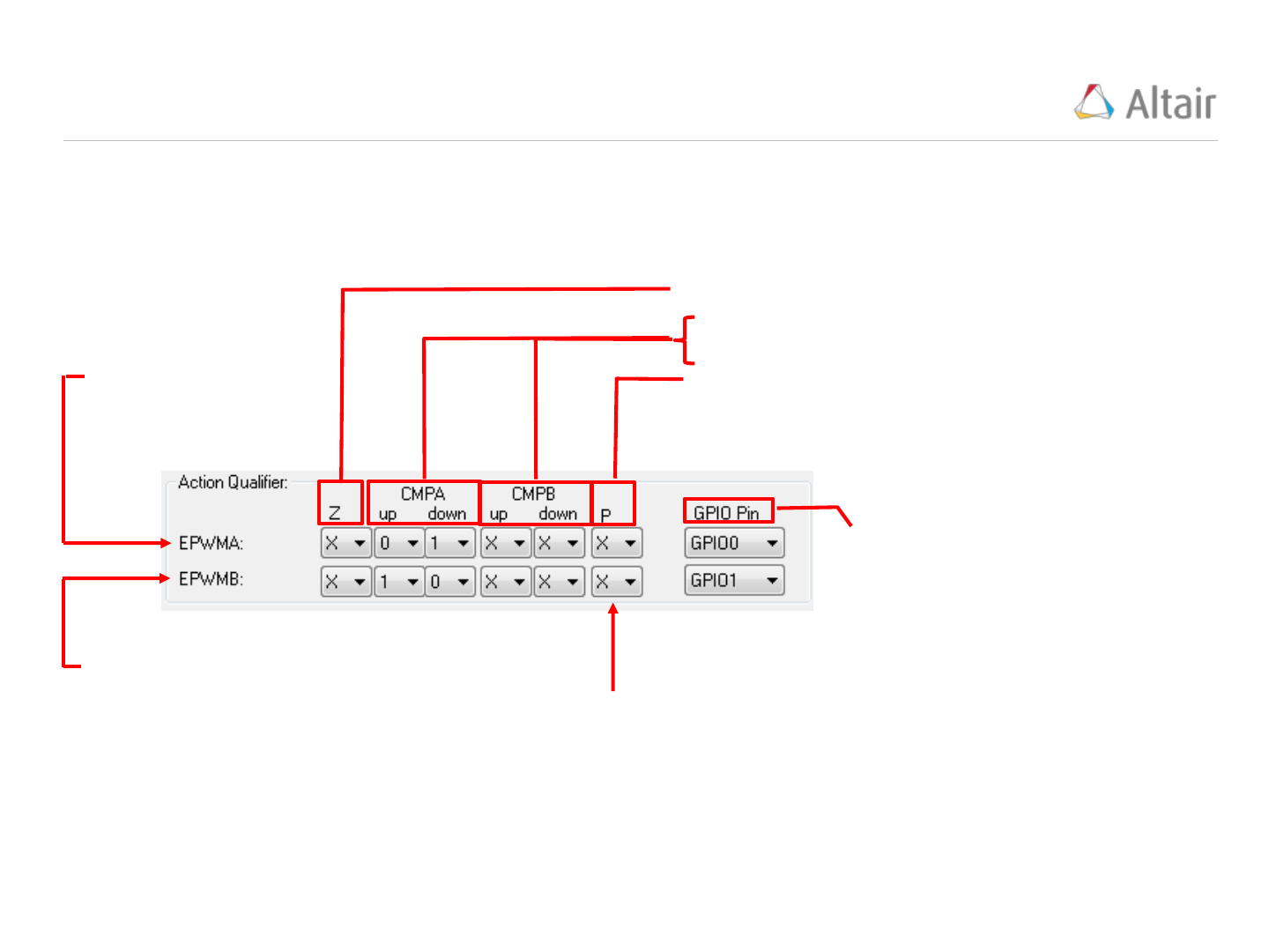
VisSim ePWM – Action Qualifier Module
20
The “Action Qualifier” Module features (Events, Actions, and PWMA and PWMB output pins) are
configured “Action Qualifier” frame of the ePWM properties window.
User select: Action dropdown:
X = Do Nothing
0 = Force PWM output to 0
1 = Force PWM output to 1
T = Toggle PWM output
Events:
Z = When TBCTR = 0
up = When TBCTR = CMP while increasing
down = When TBCTR = CMP while decreasing
P = When TBCTR = TBPRD
Output Pin numbers
assigned to PWMA and
PWMB.
PWMA Action,
Event, & Pin
Settings
PWMB Action,
Event, & Pin
Settings
Copyright © 2015 Altair Engineering, Inc. Proprietary and Confidential. All rights reserved.
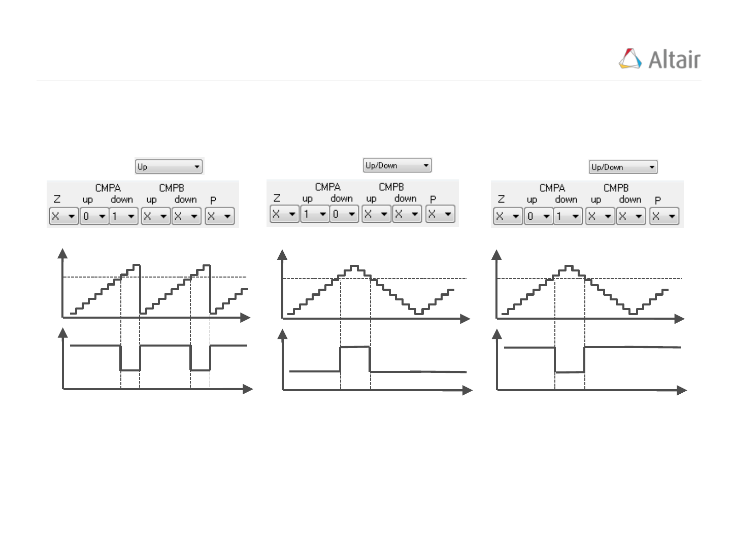
PWM Examples
21
Count Mode
Example 1
Count Mode
Count Mode
Example 2 Example 3
CMP
value
TBCTR
PWM
time
time
Copyright © 2015 Altair Engineering, Inc. Proprietary and Confidential. All rights reserved.
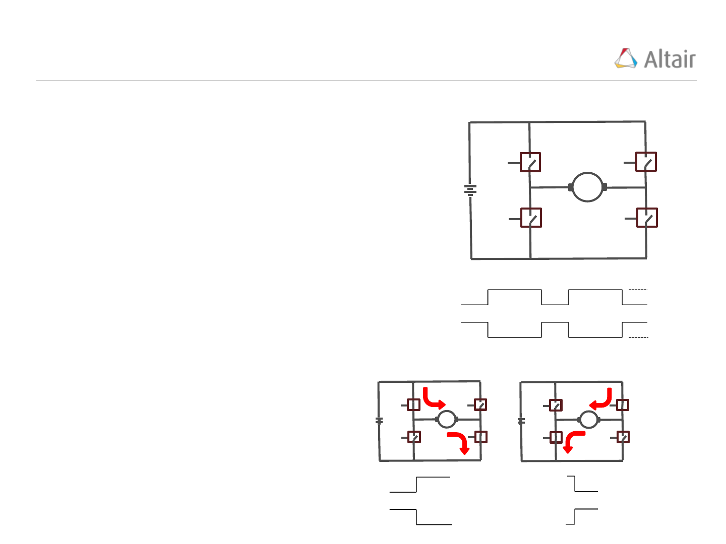
PWM Deadband
22
An H bridge is an electronic circuit consisting of 4 switches. One use of an H bridge is to provide
bidirectional rotation control of a DC motor.
When switches S1 and S4 are closed (and S2 and S3
are open) a positive voltage is applied across the motor
(M) causing it to rotate in one direction. Closing S3 and
S2 and opening S1 and S4 reverses the voltage polarity
across the motor causing it to operate in the reverse
direction.
S1
S2
S3
S4
+
Vdc
-
M
The four switches are controlled by a complimentary
pair of PWM signals, PWMA and PWMB. PWMA
controls S1 and S4 and PWMB controls S2 and S3. An
ideal pair of PWM control signals is shown to the right:
Closed
PWMA
PWMB
Closed
Open
Open
Ideal switches require 0 time to switch
between states (Open and Closed). If
the switches are ideal, two current flow
patterns are possible:
Closed
PWMA
PWMB
Closed
Open
Open
PWMA
PWMB
S1
S2
S3
S4
S1
S2
S3
S4
Copyright © 2015 Altair Engineering, Inc. Proprietary and Confidential. All rights reserved.
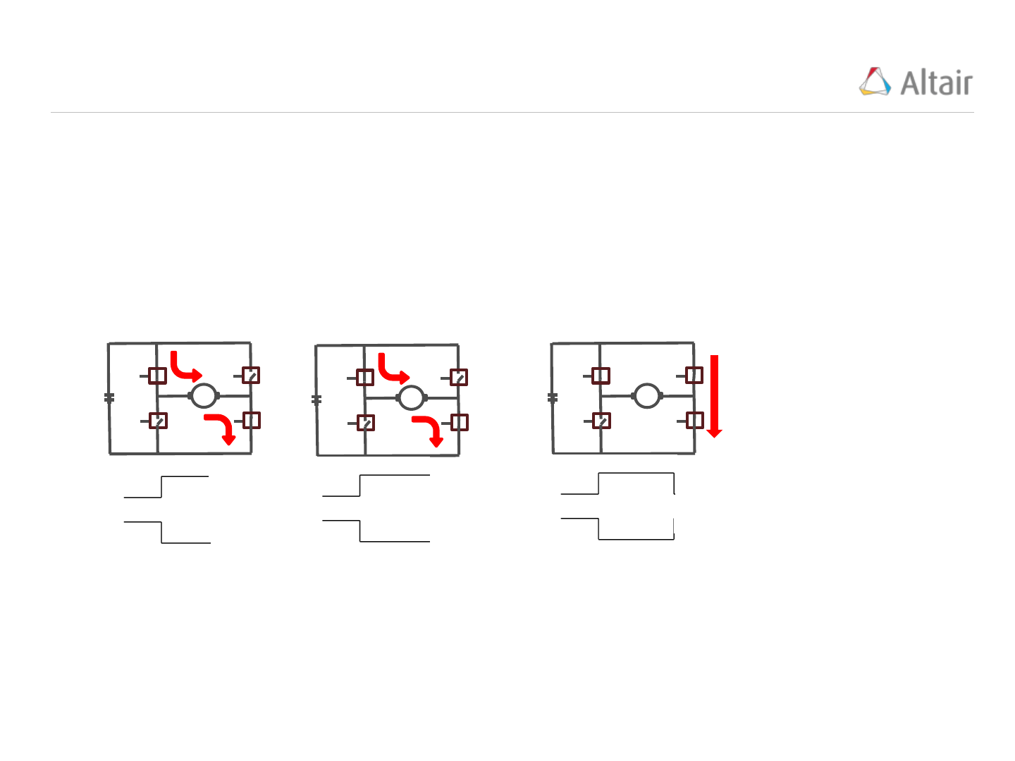
PWM Deadband – Shoot Through
23
PWMA commanded S1
and S4 to Open but
due to their longer
switch “turn Off” times,
they remain closed
while S3 (commanded
by PWMB) closes
because of it’s shorter
“turn On” time*.
Real switches (Thyristors, FET’s, …) do not behave in an ideal manner. They have a finite “turn On” and
“turn Off” switch transition time which, in general, are not equal. When these switches are used in an H
bridge under PWM control, these transition times can cause a catastrophic failure of the switches called
“Shoot Through”. For example, a thyristor application may have a “turn On” = .2 milliseconds and “turn
Off” = 2.8 milliseconds.
In the following sequence of switch conditions, PWMA transitions from ON (Closed) to OFF (Open) and
PWMB from OFF to ON. The sequence uses non-ideal switches, each with a “turn Off” time > “turn On”
time.
Closed
PWMA
PWMB
Open
Closed
PWMA
PWMB
Open
Closed
PWMA
PWMB
Open
S1
S2
S3
S4
S1
S2
S3
S4
S1
S2
S3
S4
PWM signal generators have a feature called “Deadband” which provides a method for independently
adding delay to the PWMA and PWMB edges (both rising and falling edges) to accommodate switch
transition times and prevent a Shoot Through situation from occurring.
* S2 was excluded in this explanation for clarity, it too could be in a closed state.
Copyright © 2015 Altair Engineering, Inc. Proprietary and Confidential. All rights reserved.
PWMB
PWMA
DbB
DbA
PWMB
PWMA
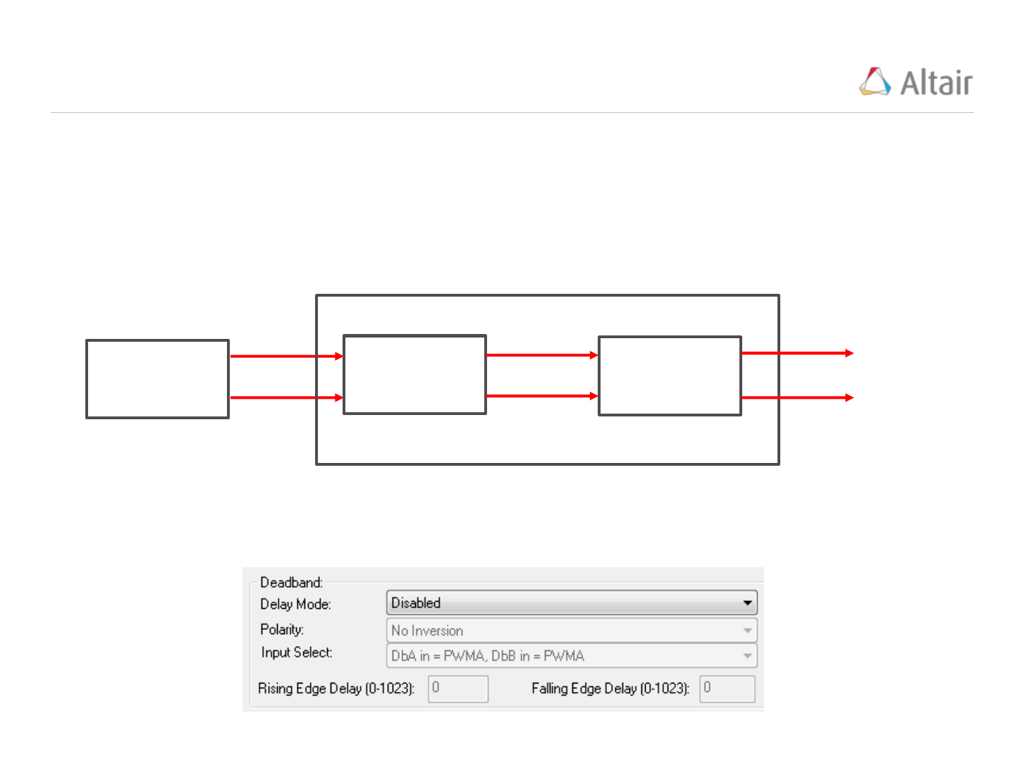
VisSim ePWM – Deadband Module
24
The “Deadband” Module allows delays to be added to rising and/or falling edges of the PWM signals.
The input signals to the “Deadband” module are the PWMA and PWMB output signals from the “Action
Qualifier” module. Internally, the “Deadband” module creates the signals “DbA” and “DbB” for channel
A and B based on the “Input Select” settings. The “Delay Mode” and “Polarity” settings are then
applied to the “DbA” and “DbB” signals to produce the PWMA and PWMB output signals (below):
Action Qualifier
Module
Deadband Module
Input Select
Delay Mode
And Polarity
The “Deadband” Module of the ePWM (“Embedded/F280x”) block is located in the "Deadband" frame
of the ePWM properties window.
Copyright © 2015 Altair Engineering, Inc. Proprietary and Confidential. All rights reserved.
VisSim ePWM – Deadband Module
25
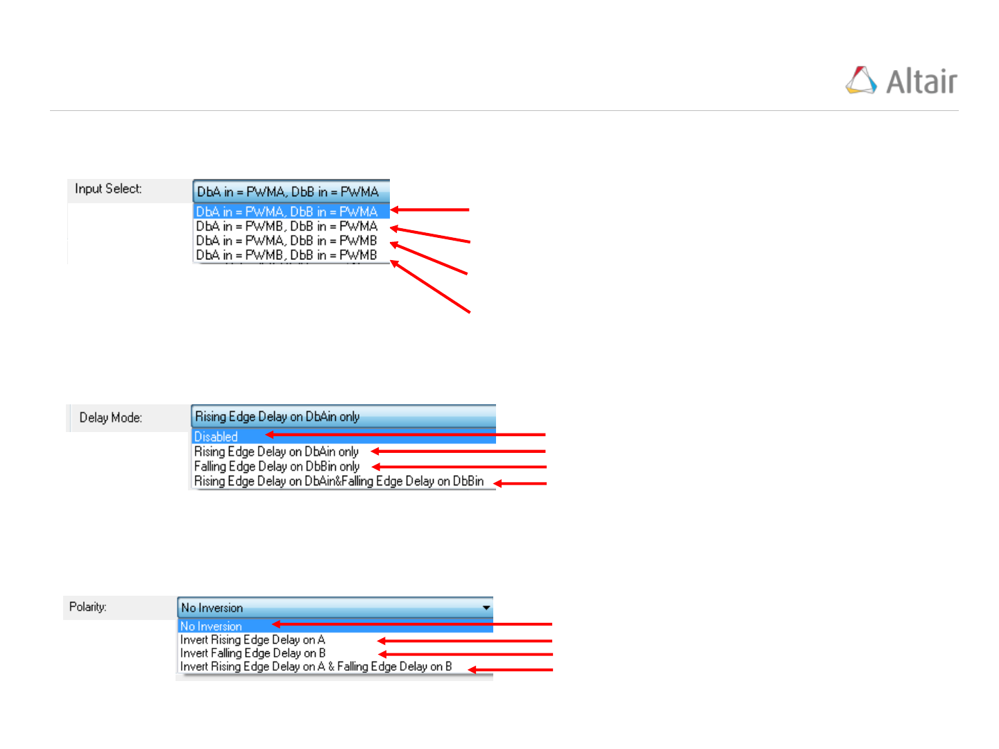
• Off
• Deadband is applied to PWMA rising edge
• Deadband is applied to PWMB falling edge
• Deadband is applied to PWMA rising edge and
PWMB falling edge
Delay Mode: Specifies the PWM Deadband mode to be used for Deadband operations, there
are four options:
• Off
• Invert rising edge delay on PWMA
• Invert falling edge delay on PWMB
• Invert rising edge delay on PWMA and invert falling
edge delay on PWMB
Polarity: The polarity control allows you to specify whether the rising-edge delayed signal and/or the
falling-edge delayed signal is to be inverted before being sent out of the Deadband module. There are
four options
• PWMA In is the source for both falling-edge and rising-edge
delay. This is the default mode.
• PWMA In is the source for falling-edge delay, PWMB In is the
source for rising-edge delay.
• PWMA In is the source for rising edge delay, PWMB In is the
source for falling-edge delay.
• PWMB In is the source for both falling-edge and rising-edge
delay.
Input Select: Specifies the PWM source signals to be used for ChA and ChB deadband operations.
These signals are named “DbA” and “DbB”. Four configuration options are available
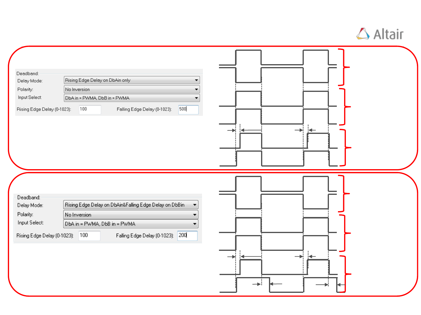
Copyright © 2015 Altair Engineering, Inc. Proprietary and Confidential. All rights reserved.
200 counts
100 counts
DbA
DbB
PWMB
PWMA
VisSim ePWM – Deadband Module Examples
26
PWMA
PWMB
PWM input signals
from Action Qualifier
Module
PWM signals after
Input Select
PWM output signals
from Deadband
Module
Example 1:
100 counts
DbA
DbB
PWMB
PWMA
PWMA
PWMB
PWM input signals
from Action Qualifier
Module
PWM signals after
Input Select
PWM output signals
from Deadband
Module
Example 2:
Copyright © 2015 Altair Engineering, Inc. Proprietary and Confidential. All rights reserved.
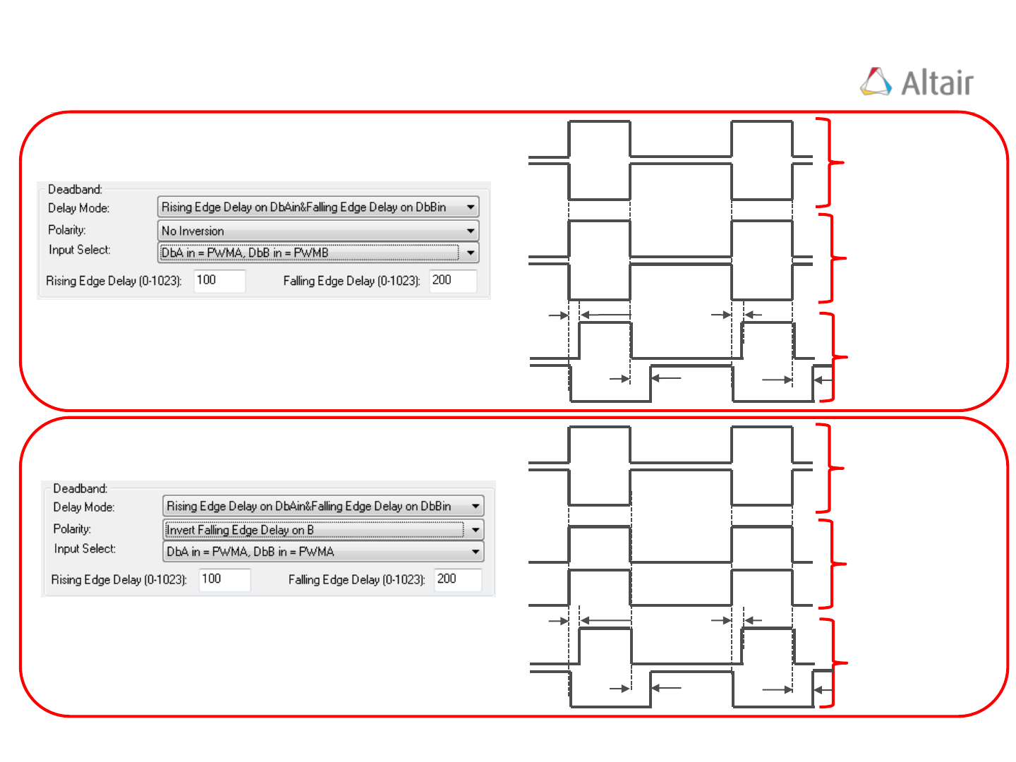
200 counts
100 counts
DbA
DbB
PWMB
PWMA
VisSim ePWM – Deadband Module Examples
27
PWMA
PWMB
PWM input signals
from Action Qualifier
Module
PWM signals after
Input Select
PWM output signals
from Deadband
Module
Example 3:
100 counts
DbA
DbB
PWMB
PWMA
PWMA
PWMB
PWM input signals
from Action Qualifier
Module
PWM signals after
Input Select
PWM output signals
from Deadband
Module
Example 4:
200 counts

Copyright © 2015 Altair Engineering, Inc. Proprietary and Confidential. All rights reserved.
VisSim ePWM – Event Time Module
28

Copyright © 2015 Altair Engineering, Inc. Proprietary and Confidential. All rights reserved.
VisSim ePWM – Fault Handling
29
Copyright © 2015 Altair Engineering, Inc. Proprietary and Confidential. All rights reserved.
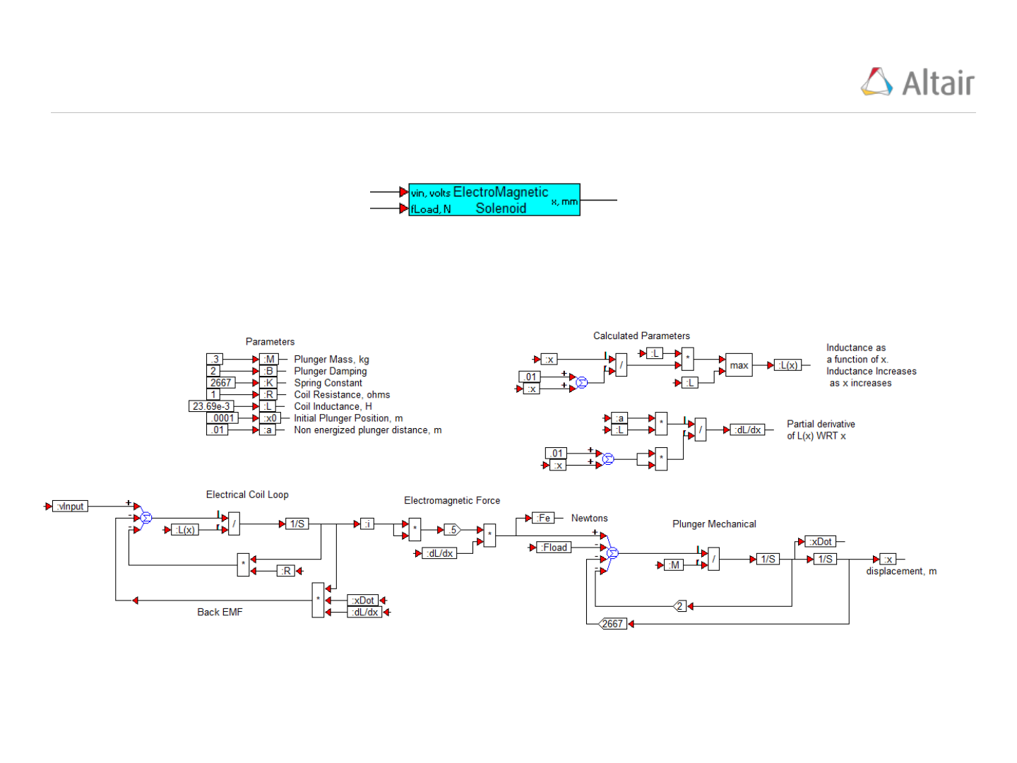
PWM Example – Solenoid Control
30
Solenoid Model (Top Level):
Solenoid Model (Details):
Copyright © 2015 Altair Engineering, Inc. Proprietary and Confidential. All rights reserved.
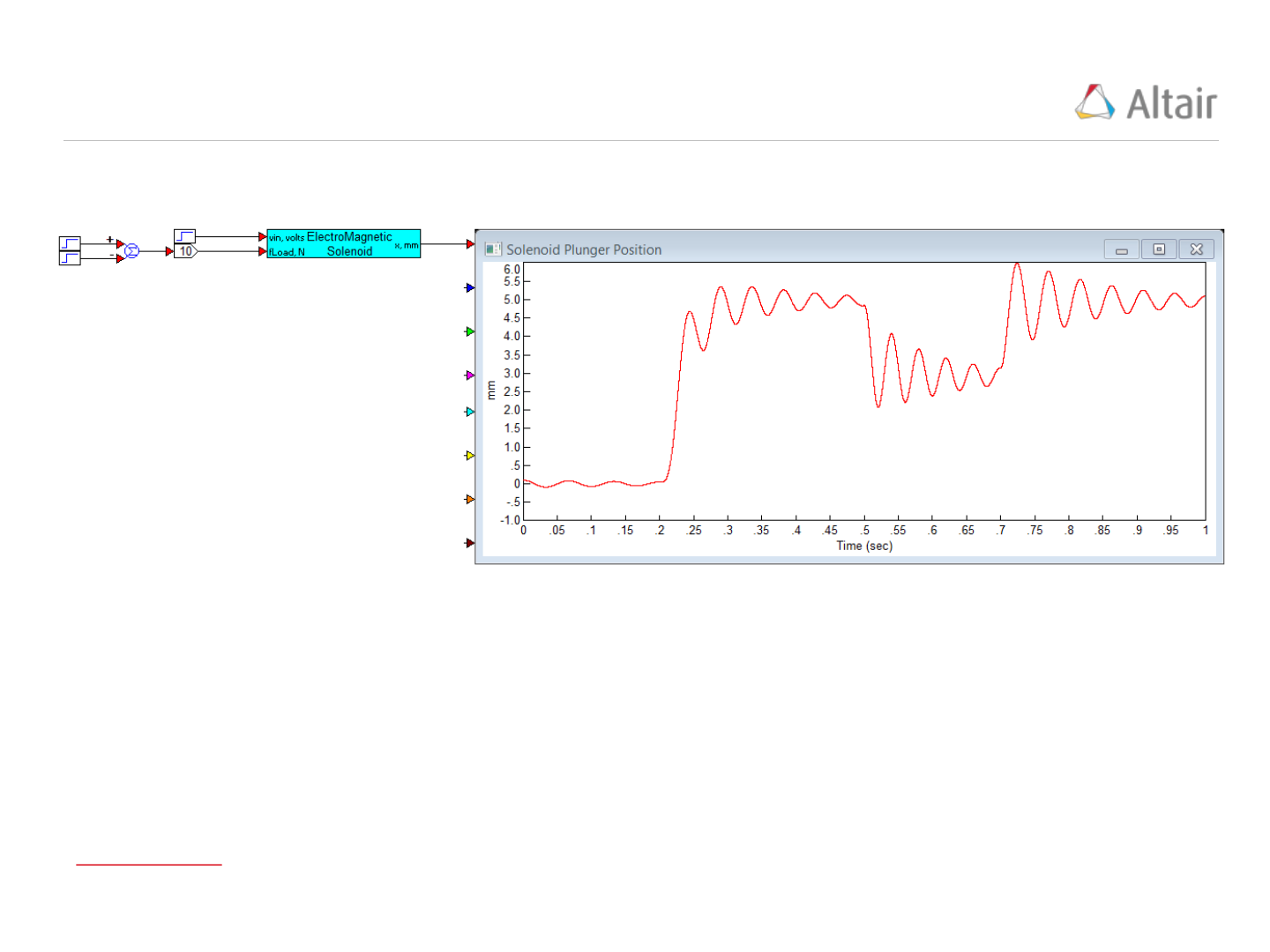
PWM Example – Solenoid Simulated Response
31
Solenoid Model Simulation Response:
Vin = 5 volts applied at 0.2 seconds
fLoad = 10 Newtons applied at 0.5 seconds and removed at 0.7 seconds
Simulation Update Time = 1e-5 seconds
Solenoid Model
Copyright © 2015 Altair Engineering, Inc. Proprietary and Confidential. All rights reserved.
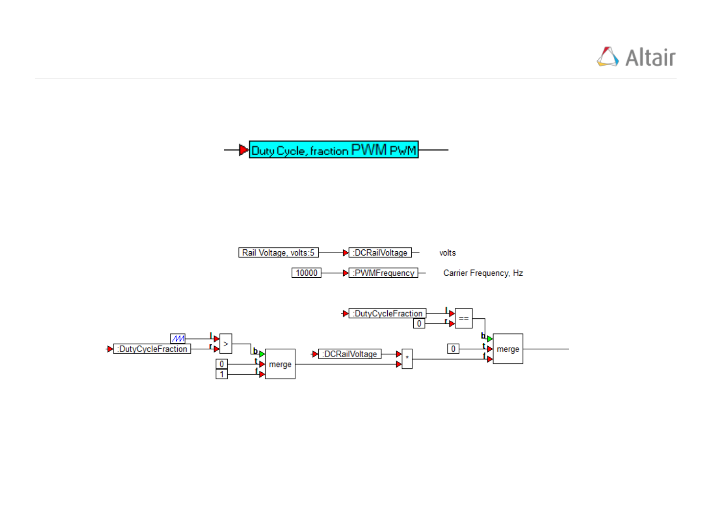
PWM Example – Solenoid PWM Generator
32
PWM Model (Top Level):
PWM Model (Details):
Copyright © 2015 Altair Engineering, Inc. Proprietary and Confidential. All rights reserved.
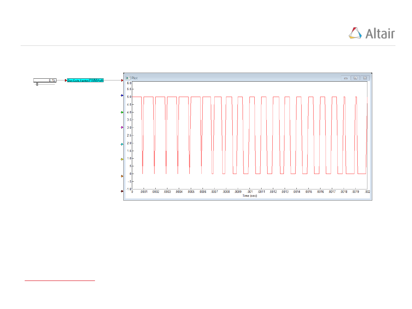
PWM Example – Solenoid PWM Generator Simulation
33
PWM Model Simulation Results:
PWM Carrier Frequency = 10kHz
Duty Cycle Slider swept from .8 to .15 during the .002 second simulation
Simulation Update Time = 1e-5 seconds
PWM Generator Model
Copyright © 2015 Altair Engineering, Inc. Proprietary and Confidential. All rights reserved.
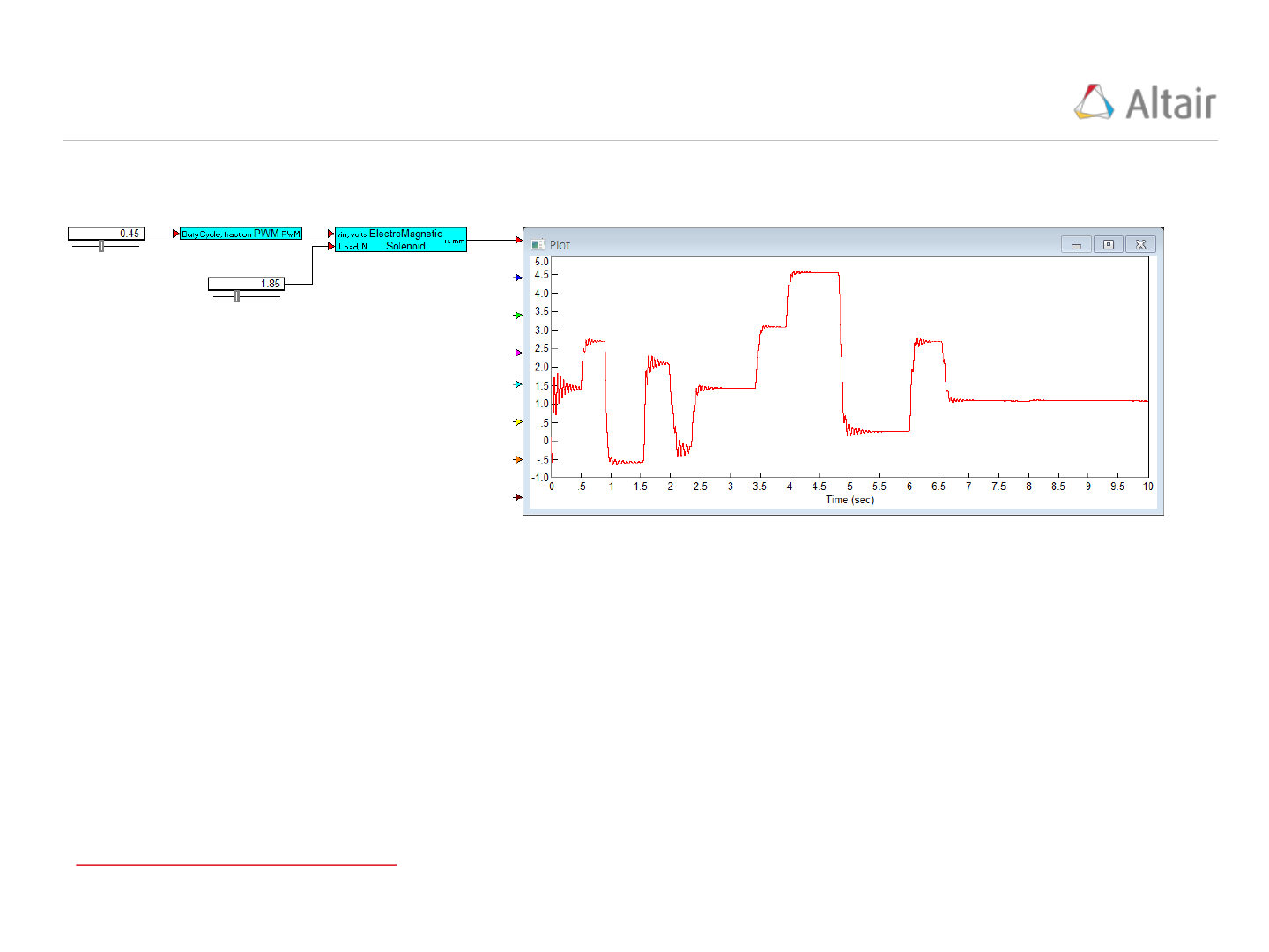
PWM Example – Solenoid w/PWM Control Simulation
34
Solenoid w/PWM Control Simulation Results:
PWM Carrier Frequency = 10kHz
Duty Cycle Slider swept randomly between 0 and 1 during the 10 second simulation
Simulation Update Time = 1e-5 seconds
Solenoid Model with PWM Control
Copyright © 2015 Altair Engineering, Inc. Proprietary and Confidential. All rights reserved.
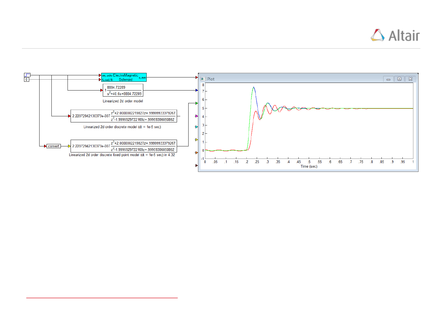
PWM Example – Solenoid Approximate Transfer Function
35
Solenoid Approximate Fixed Point Transfer Function
Vin = 5 volts
Fload = 0 Newtons
Simulation Update Time = 1e-5 seconds
Solenoid Approximate Transfer Function Model
Copyright © 2015 Altair Engineering, Inc. Proprietary and Confidential. All rights reserved.
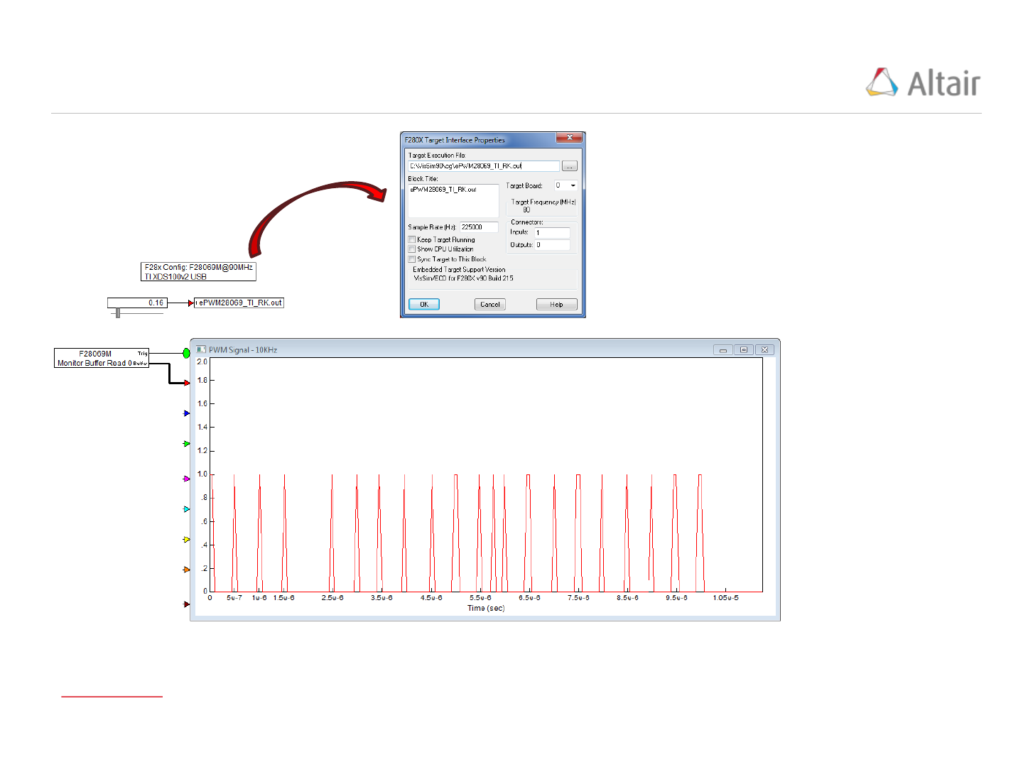
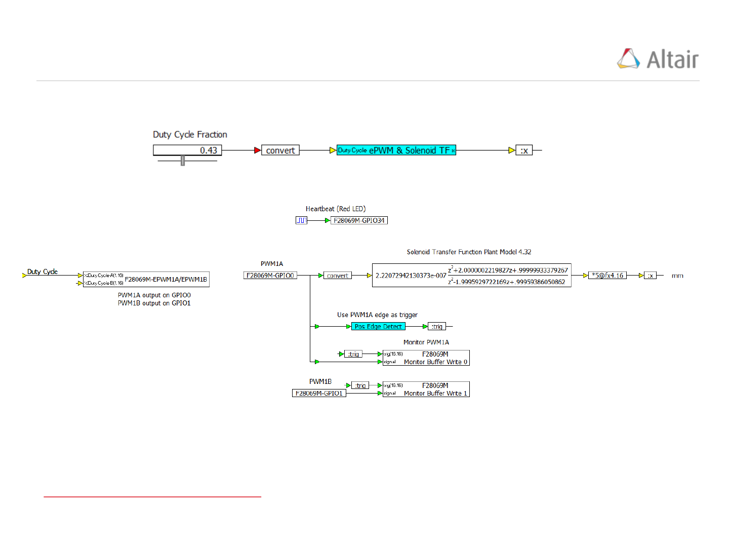
PWM Example – Solenoid PIL PWM Configuration
37
PWM Configuration
Carrier Frequency = 10kHz
GPIO0 = PWM 1A output
GPIO1 = PWM 1B output

Copyright © 2015 Altair Engineering, Inc. Proprietary and Confidential. All rights reserved.
PWM Example – Motor Control
40
It is important to understand how the PWM Carrier Period (and Frequency) is selected.
To do this we will create a basic motor model, identify its fundamental time constant, and then select
the PWM Carrier Period short enough to produce an acceptable level of motor velocity fluctuation.
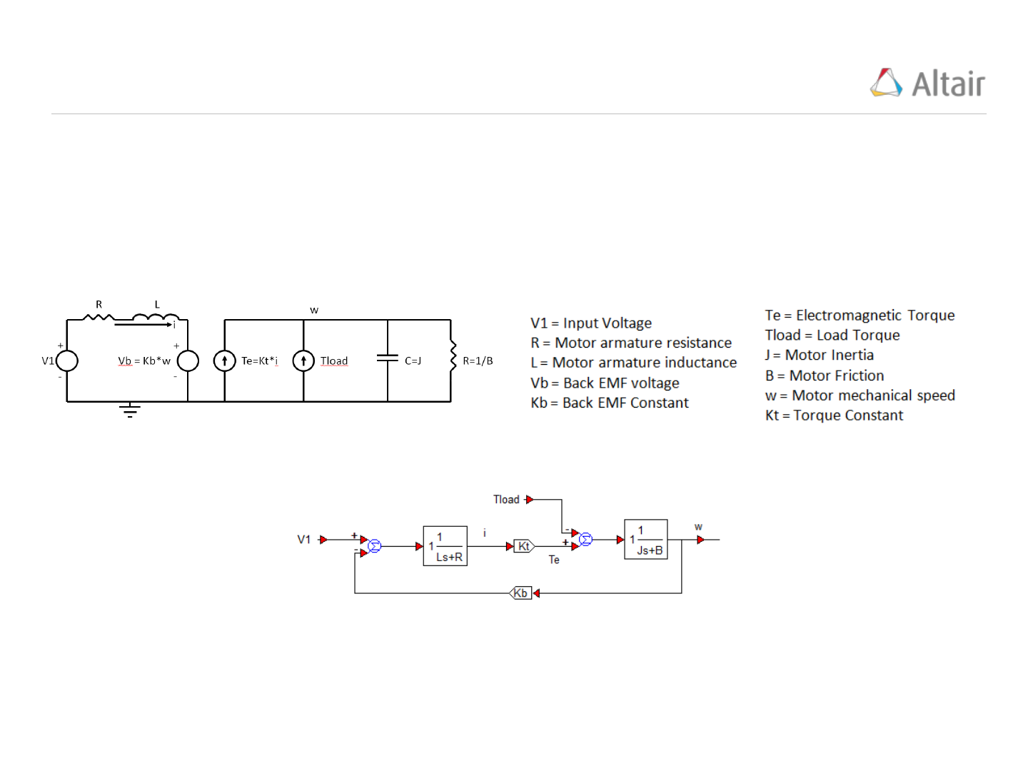
Basic Motor Model:
Where:
The equivalent motor block diagram becomes:
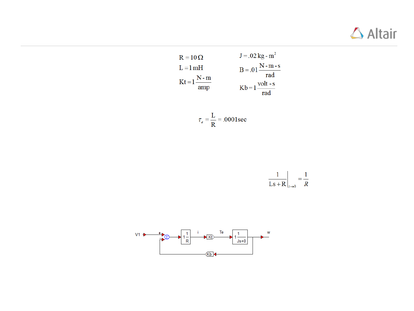
Copyright © 2015 Altair Engineering, Inc. Proprietary and Confidential. All rights reserved.
Motor Dynamics – Electrical Time Constant
41
Using the following example values;
The Electrical Time Constant is calculated as:
To calculate the Mechanical Time Constant, the following simplifications are applied;
Tload = 0 (no load torque)
Motor friction, B = 0
And the electrical dynamics are replaced by their dc-value;
Applying these assumptions, the motor model block diagram simplifies to:
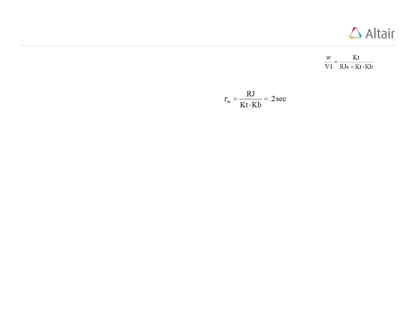
Copyright © 2015 Altair Engineering, Inc. Proprietary and Confidential. All rights reserved.
Motor Dynamics – Mechanical Time Constant
42
The closed loop transfer function of the simplified motor model is calculated as:
And the Mechanical Time Constant is calculated as:
In successful applications, the Mechanical Time Constant should be the fundamental (or dominant)
time constant, typically 100 to 1000 times slower than the electrical time constant.
Copyright © 2015 Altair Engineering, Inc. Proprietary and Confidential. All rights reserved.
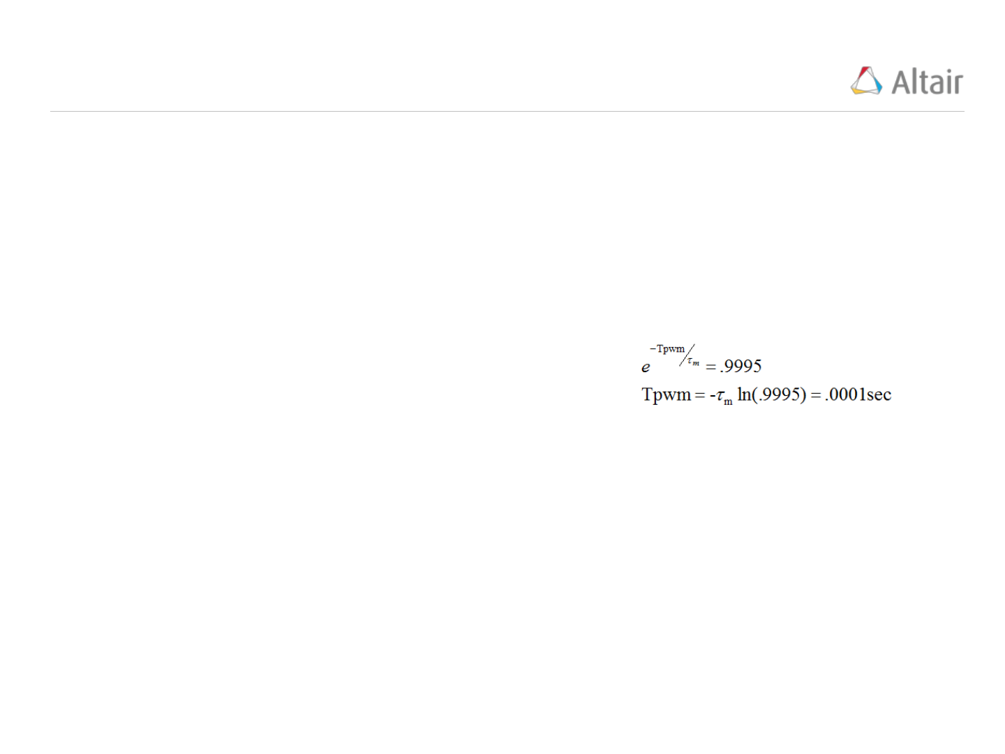
PWM Carrier Period & Frequency
43
The PWM Carrier Period, Tpwm, and Frequency, Fpwm, is calculated to produce an acceptable value
of motor velocity fluctuation.
As an example, assume that a 0.05% velocity fluctuation is the goal.
If the initial motor velocity, w(0) = 1, and the dominant time constant of the motor = mechanical time
constant is 0.2 seconds,
Then the problem is that of solving the mechanical time
constant for the Tpwm (PWM Carrier Period):
Fpwm = 1/Tpwm = 10KHz.
The typical range for the PWM Carrier Frequency is 10KHz <= Fpwm <= 40KHz. Using frequencies
less than 10KHz result in unacceptable motor velocity ripple and values greater than 40KHz tend to
increase the transistor switching frequency (in the H Bridge) to a level that causes them to heat up
and prematurely fail.
Copyright © 2015 Altair Engineering, Inc. Proprietary and Confidential. All rights reserved.
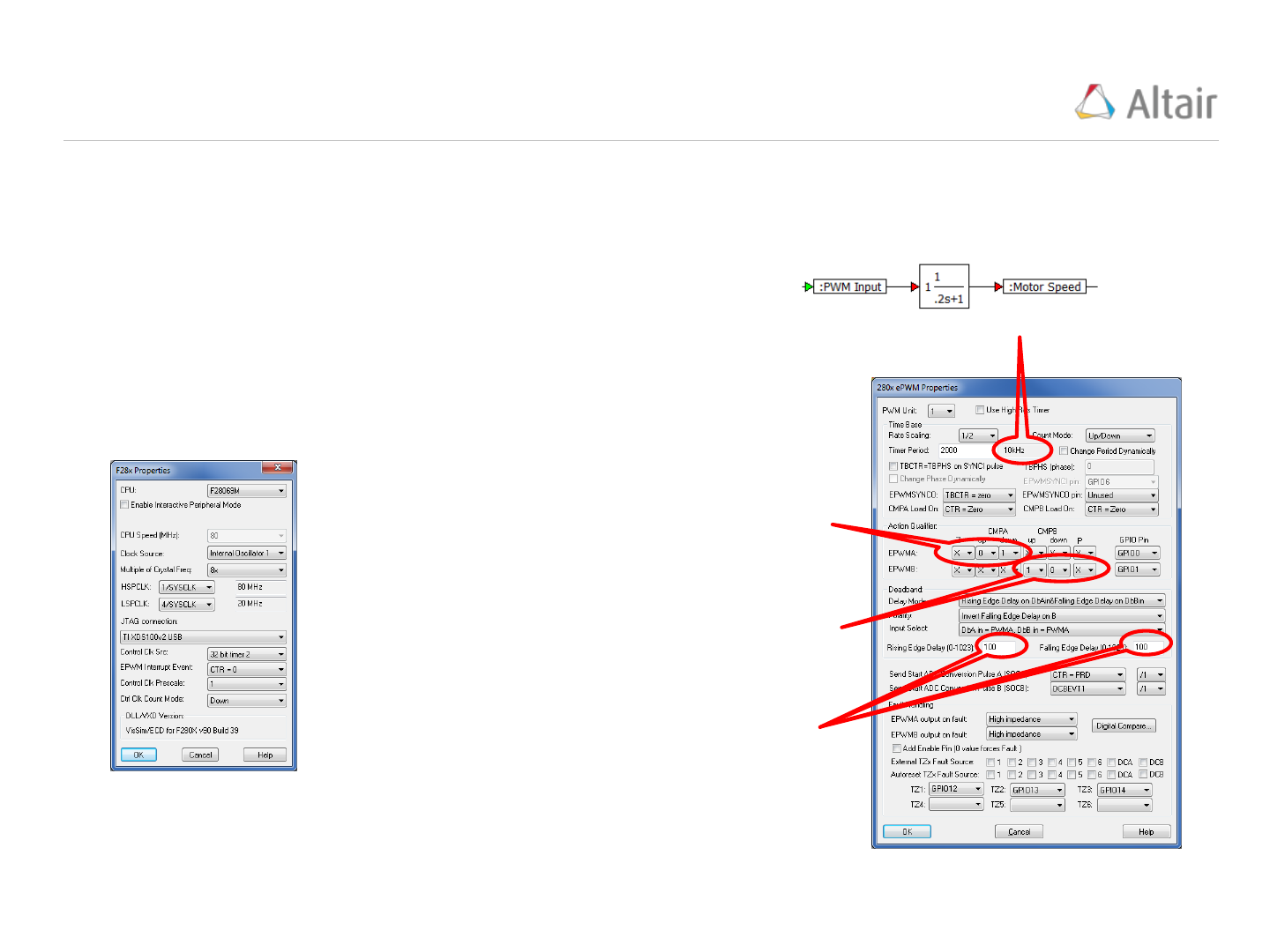
Motor Speed Response to PWM
44
This example illustrates the response of a motor transfer function model to a PWM signal implemented
on the F28069M LaunchPad target. Values from the previous “Motor Dynamics” example are used.
The motor model is defined as a unity gain first order transfer
function with a mechanical dominant time constant = .2 seconds
(right)
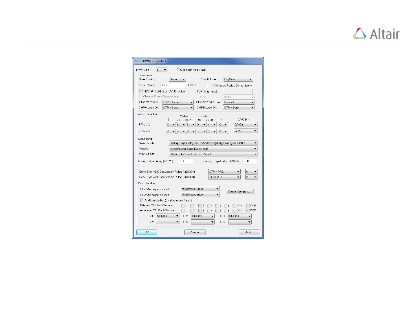
The PWM Carrier Frequency is set to 10KHz. Using the following settings:
F28x Properties: CPU Speed
(MHz) = 80MHz
ePWM Properties:
Rate Scaling = 1/2
Count Mode = up/down
Timer Period = 2000
Since the PWM Carrier Frequency is 10KHz, the target model update frequency is selected to be
20 times faster (200KHz), this is equivalent to a target update time = 1/200KHz = 5e-6 sec.
PWM Carrier Frequency
if counting “up” and TBCTRB goes thru
CMPB, set EPWMB = 1
if counting “down” and TBCTRB goes
thru CBMPB, set EPWMB = 0
if counting “up” and TBCTRA goes thru
CMPA, set EPWMA = 0
if counting “down” and TBCTRA goes
thru CMPA, set EPWMA = 1
Rising and Falling edge deadbands (time
delays) normally set to the same value
(units are ticks)
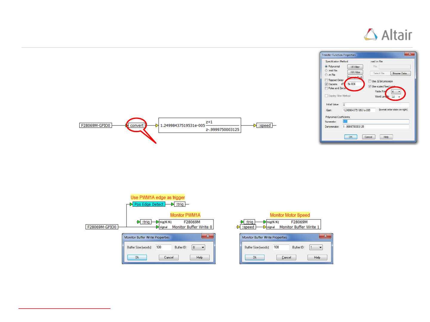
Copyright © 2015 Altair Engineering, Inc. Proprietary and Confidential. All rights reserved.
Motor Speed Response – Motor Model
45
The motor model transfer function is converted to a fixed point discrete
transfer function, format 4.32, using an update time = 5e-6 sec (right)
Format 4.32, same as the transfer function
The motor model transfer function receives the PWMA signal from
GPIO0 (below) NOTE: PWMB is not used in this example.
Monitor Buffers are used to record 100 elements of PWM data (into Monitor Buffer 0) and Motor
speed (into Monitor Buffer 1) – (below):
The trigger signal “:trig” is pulsed every time a PWM cycle begins (10KHz)
View source model in VisSim
Copyright © 2015 Altair Engineering, Inc. Proprietary and Confidential. All rights reserved.
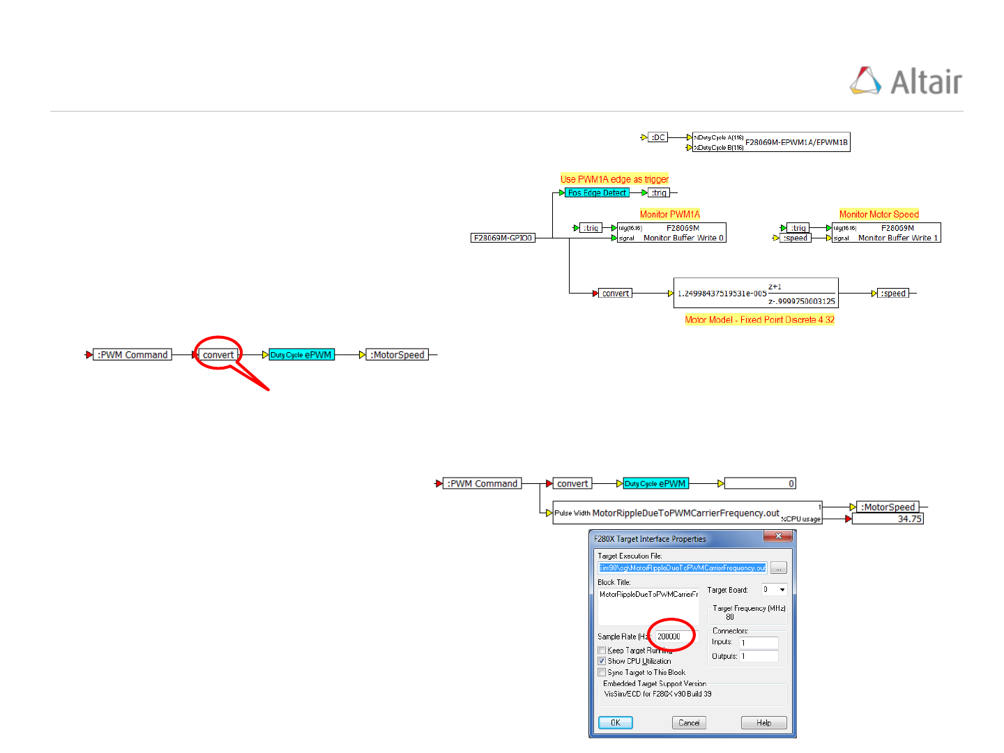
Motor Speed Response – Source Model
46
The completed Source model becomes
(right):
Format 1.16 required as the duty cycle command value for the ePWM block
C Code is generated for “ePWM” and compiled into “MotorRippleDueToPWMCarrierFrequency.out”
by applying the “Code Gen…” option under the “Tools” menu.
The source model is captured in a
compound block named “ePWM” (below):
The Debug model is created from the
Source model by replacing the “ePWM”
compound block with a “TargetInterface”
block configured to read the “.out” file
produced by the Source model. The
“TargetInterface” is configured to execute
at a “Sample Rate (Hz):” = 200KHz rate
(right):
Copyright © 2015 Altair Engineering, Inc. Proprietary and Confidential. All rights reserved.
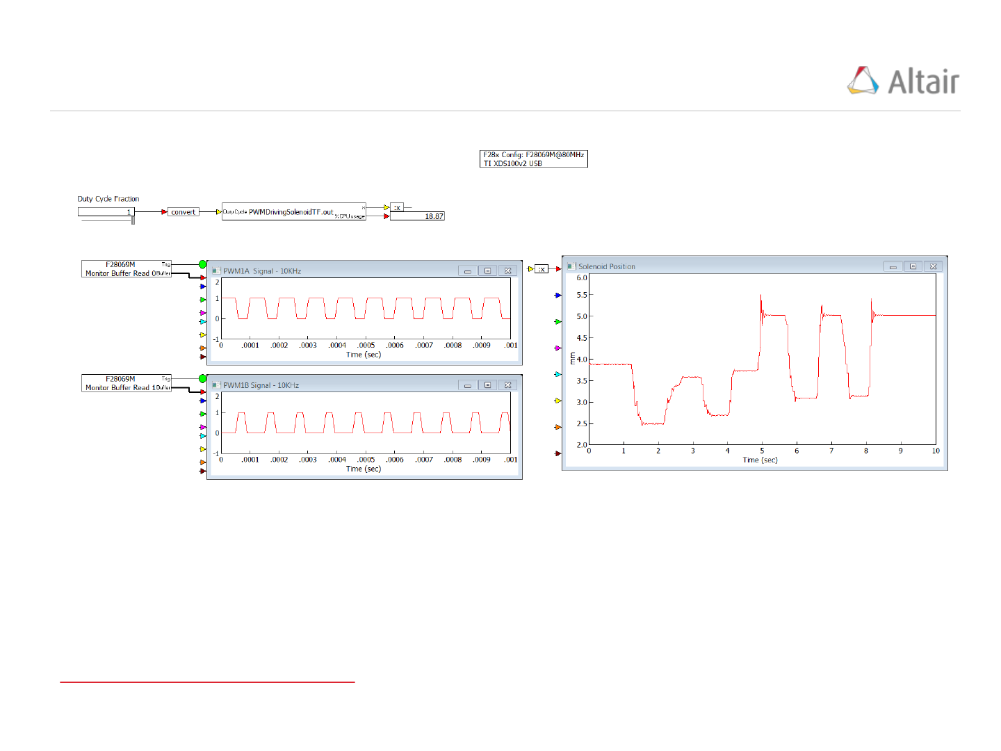
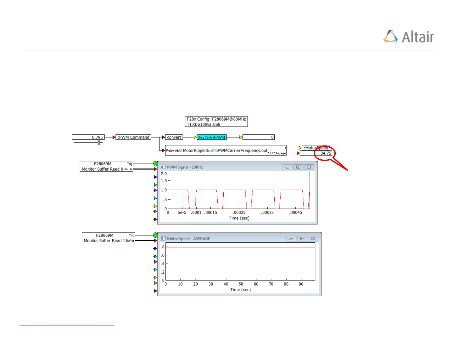
Motor Speed Response – Debug Model
47
The VisSim Debug model, which includes the “TargetInterface” block, is configured to execute at a 0.01
second update time allowing the JTAG interface adequate time to transfer the Monitor Buffer contents.
The competed Debug model and results showing the PWM signal and the motor speed buffers are
presented below:
Fixed Point motor model
transfer function % CPU
utilization.
NOTE: this model would not
execute at the 200KHz rate if
Fixed Point were NOT used.
NOTE: Debug model settings: dt = 0.01 seconds, "End(sec)" = 25;
"Run in Real Time" checked, "Auto Restart" checked, and "Retain
State" checked.
View debug model in VisSim
Copyright © 2015 Altair Engineering, Inc. Proprietary and Confidential. All rights reserved.
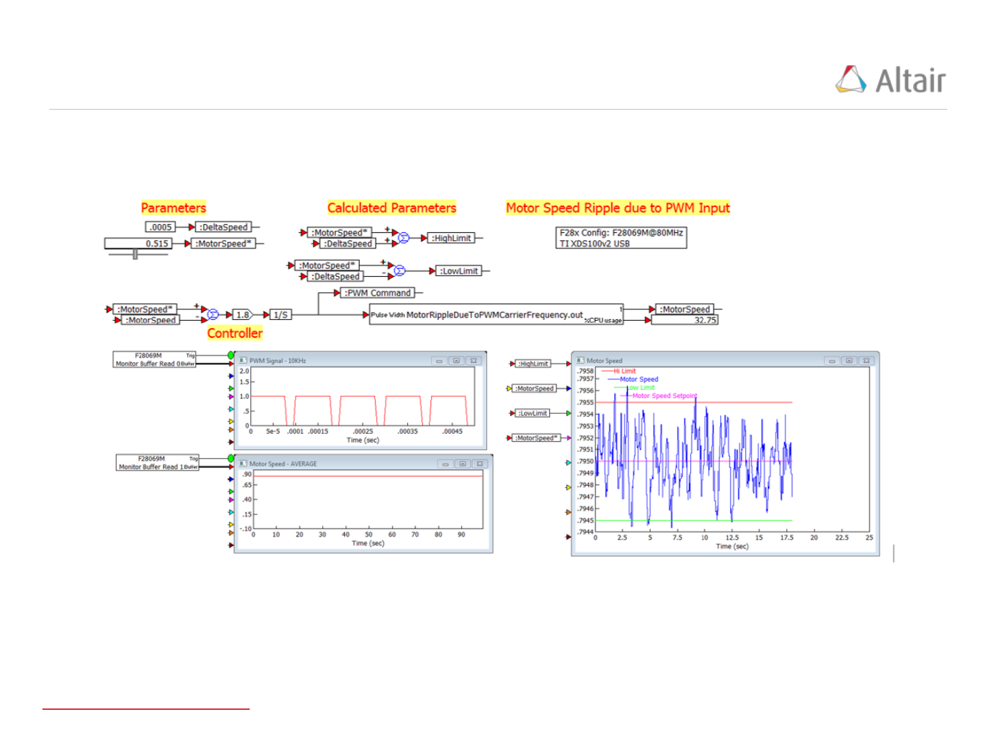
Motor Speed Response – Speed Jitter Results
48
The Debug model was allowed to restart several times with the “MotorSpeed*” fixed at .795 to
determine if the Motor Speed Jitter was within the +/- 0.0005 unit limits (below, right)
Motor Speed response to PWM is within
the +/- 0.0005 unit limits
View debug model in VisSim
Copyright © 2015 Altair Engineering, Inc. Proprietary and Confidential. All rights reserved.
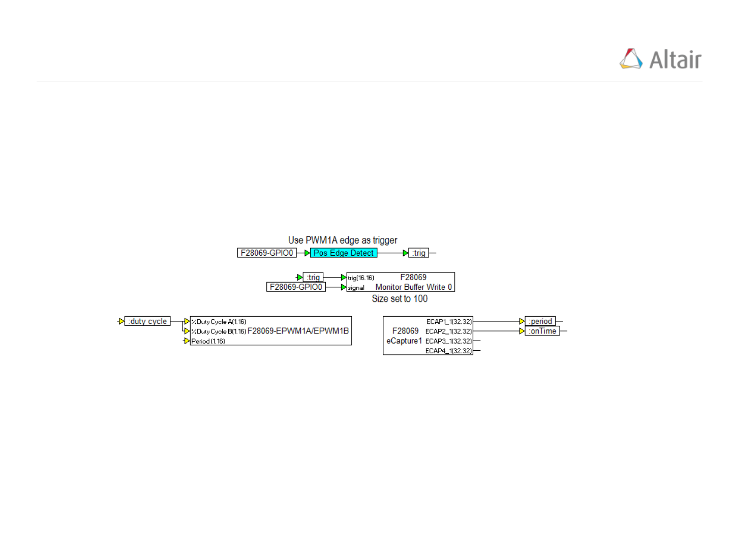
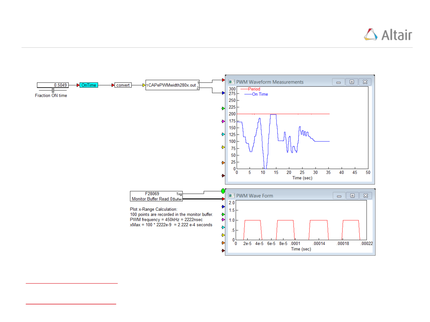
Record ePWM timing using eCap Block (1/5)
49
The “eCap” block (Embedded/Piccolo/eCap) provides the ability to record the “on” and “off” times of
PWM signals. Let’s create a VisSim model that outputs a PWM signal on GPIO0 and an “eCap” block
that records the “on” time and “period” of the PWM signal for display.
The following model is constructed. We have also included a “Monitor Buffer” to display the PWM
waveform in a “plot” block
Copyright © 2015 Altair Engineering, Inc. Proprietary and Confidential. All rights reserved.
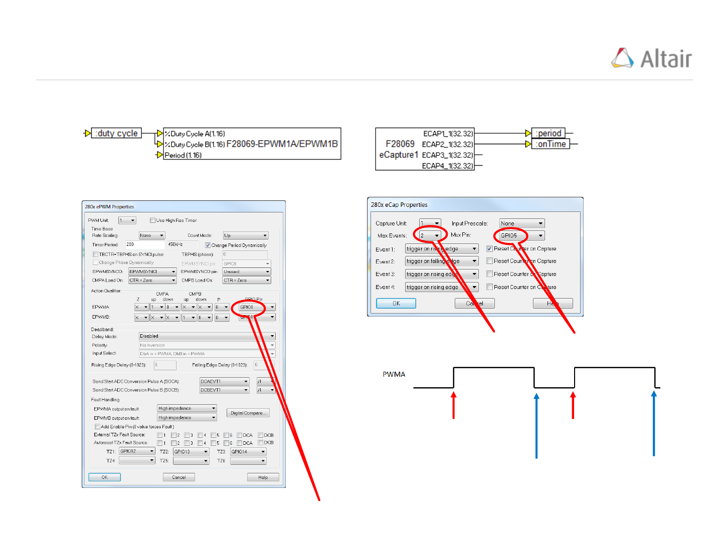
Record ePWM timing using eCap Block (2/5)
50
The “PWM” and “eCap” blocks are configured as follows:
PWM output (channel A) set to GPIO0
eCap input
set to GPIO5
Event 1
Triggers here &
timer is rest
Event 2
Triggers here
Record the
first 2 events
Copyright © 2015 Altair Engineering, Inc. Proprietary and Confidential. All rights reserved.
Record ePWM timing using eCap Block (3/5)
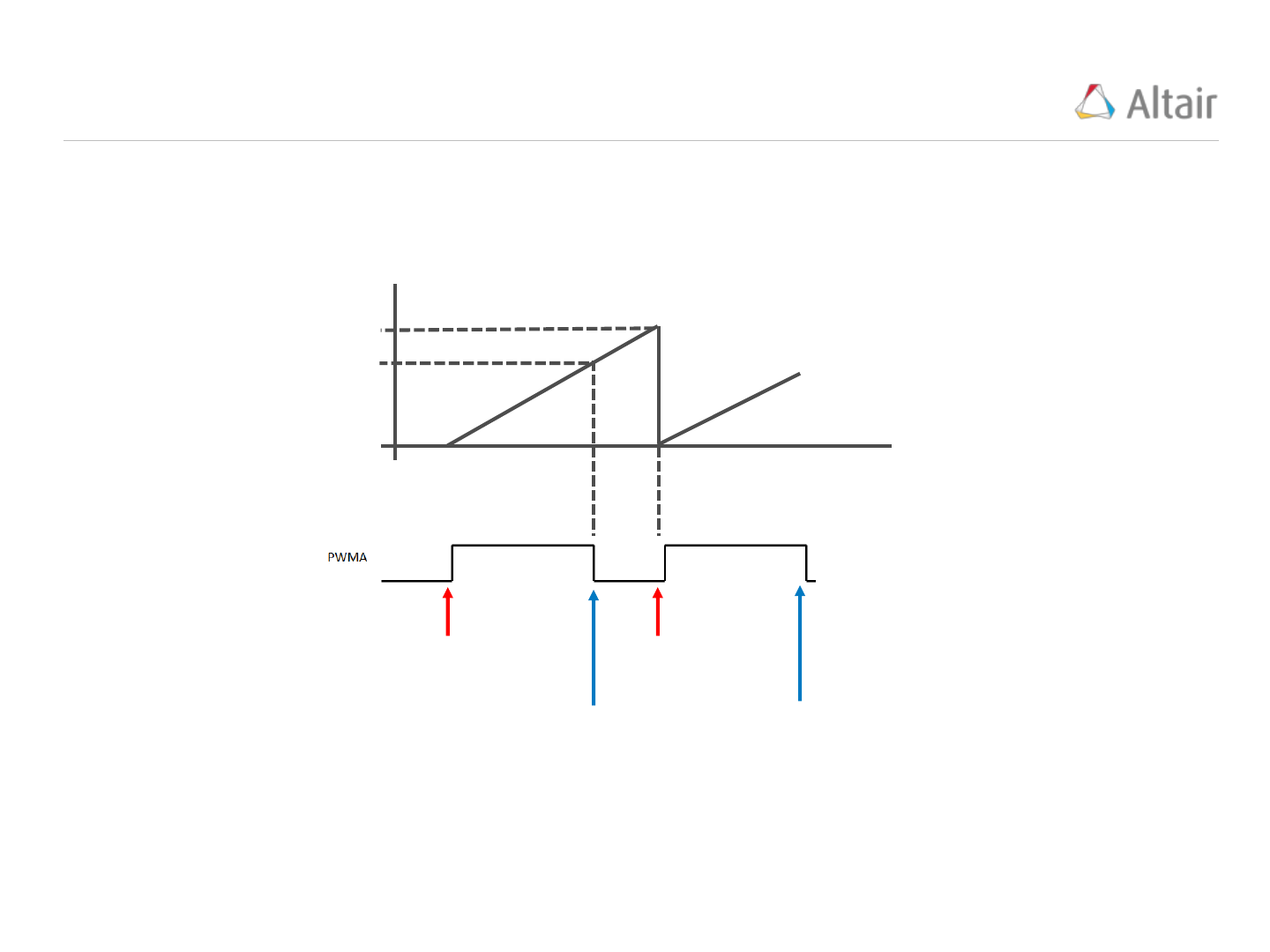
51
The “eCap” block is configured to output the values of the first 2 events. The following figure illustrates
how the event values are calculated.
Event 1
Triggers here &
timer is rest
Event 2
Triggers here
time
Timer count
Period
On time

Copyright © 2015 Altair Engineering, Inc. Proprietary and Confidential. All rights reserved.
Record ePWM timing using eCap Block (4/5)
52
For the “eCap” block to operate, we need to jumper the pins that correspond to GPIO0 and GPIO5. The
pin definitions for the F28069M LaunchPad are presented below.
The jumper is positioned as
show to the right connecting pins
35 (GPIO5) and 40 (GPIO0)
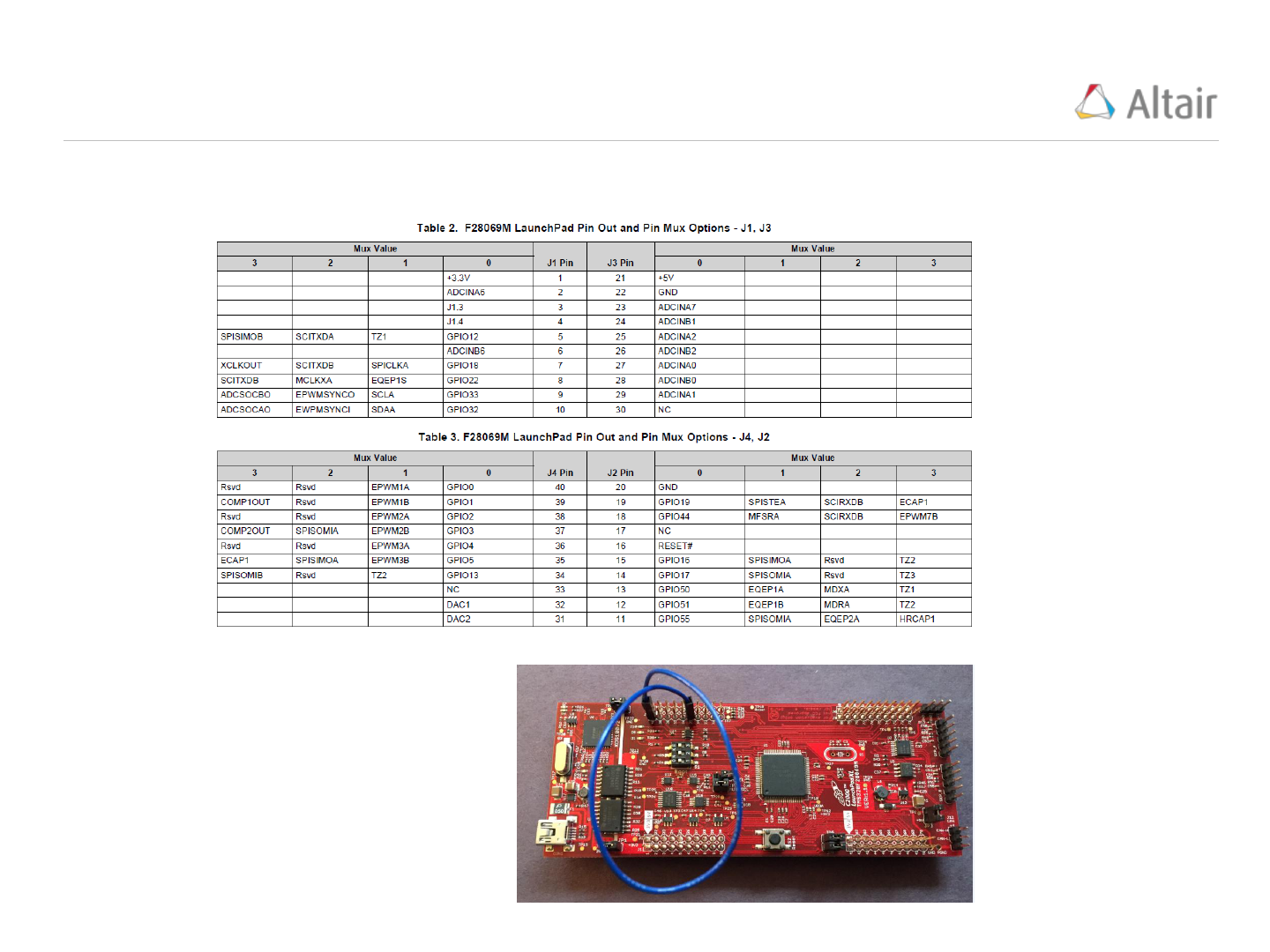
Copyright © 2015 Altair Engineering, Inc. Proprietary and Confidential. All rights reserved.
Record ePWM timing using eCap Block (4/5)
54
For the “eCap” block to operate, we need to jumper the pins that correspond to GPIO0 and GPIO5. The
pin definitions for the F28069M LaunchPad are presented below.
The jumper is positioned as
show to the right connecting pins
35 (GPIO5) and 40 (GPIO0)
Copyright © 2015 Altair Engineering, Inc. Proprietary and Confidential. All rights reserved.
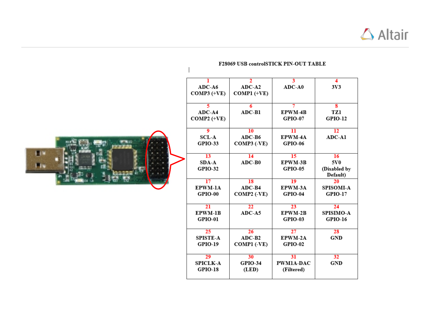
Pin Out definitions for F28069 ControlStick
55
Using the PWM and “eCap”
settings from the previous
example, the jumper settings for
the F28069 ControlStick
positioned as show to the right
connecting pins 15 (GPIO5) and
17 (GPIO0)

Copyright © 2015 Altair Engineering, Inc. Proprietary and Confidential. All rights reserved.
End of Section
56